AI for Visual Quality Inspection in PCB Manufacturing: Detect Defects Faster and Improve Yield
AI for Visual Quality Inspection in PCB Manufacturing: Detect Defects Faster and Improve Yield
PCB manufacturers face a constant challenge: catching subtle solder defects, polarity errors, or missing components before boards move to the next stage. Traditional AOI systems can miss microscopic flaws or generate false alarms—slowing throughput and increasing rework.
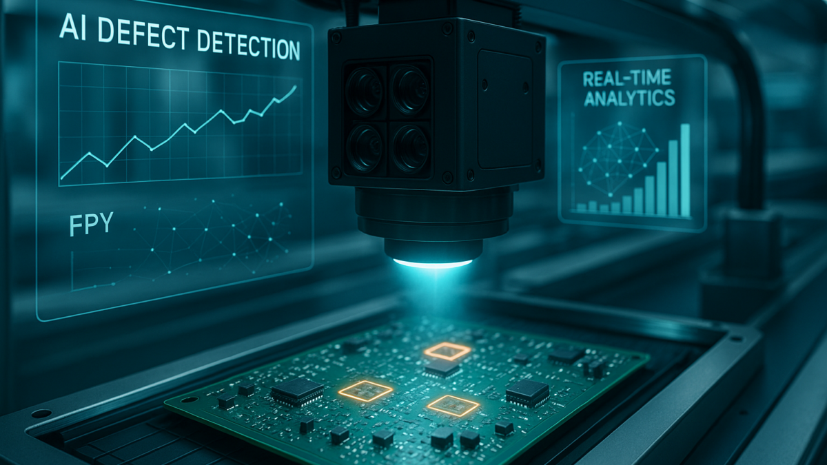
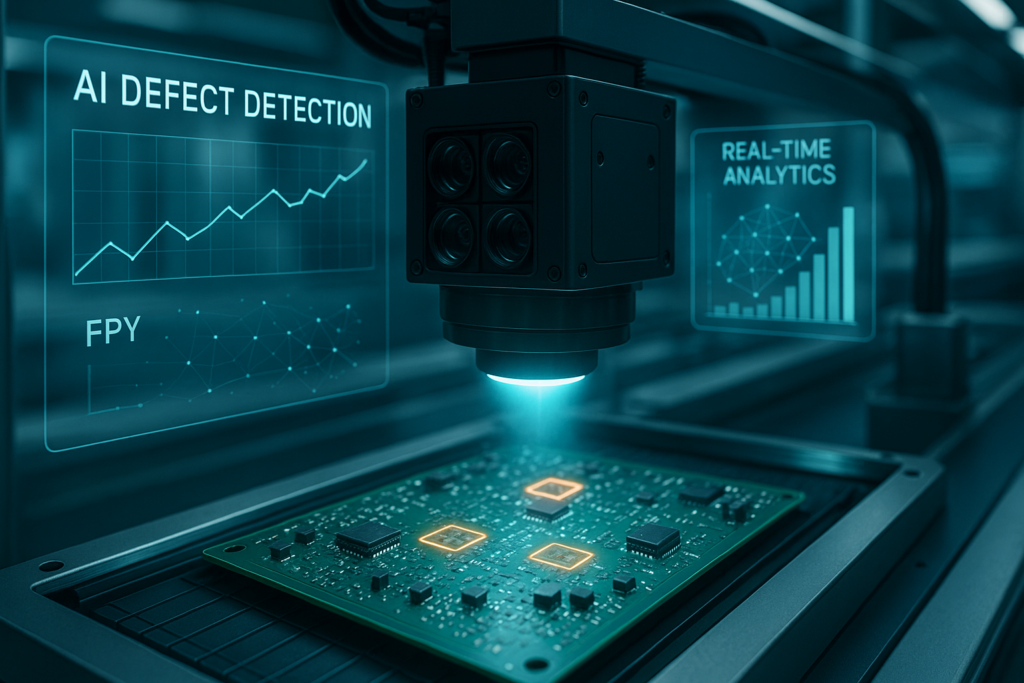
AI visual inspection in PCB manufacturing changes this by combining deep learning with real-time analytics to detect defects with high precision at production speed.
On this page
What Is AI Visual Inspection for PCB Manufacturing?
AI visual inspection uses computer vision and machine learning models trained on thousands of real images to automatically detect PCB defects—such as solder bridges, missing or misaligned components, polarity errors, scratches, and micro-cracks. Unlike fixed AOI rules, AI models keep learning and adapt to lighting, component, and layout variations, reducing false positives and missed defects.
For end-to-end visibility, connect inspection signals with line data using
SMT Analytics to monitor yield and defect trends directly from production.
Why Traditional AOI Isn’t Enough
Manual inspection challenges
- Operator fatigue and inconsistency
- Micro-defects are easily overlooked
- Variable judgment between shifts
- Slower inspection limits throughput
Rule-based AOI limitations
- Hard-coded rules struggle with real variation
- High false-call rates waste time
- Frequent reprogramming per product
- No built-in root-cause insights
Unify AOI with test outcomes via
Testing Stations Analytics to close the loop between optical findings and electrical tests.
How AI Visual Inspection Works
Cameras capture detailed PCB visuals across lines and stations.
Models trained on real images detect solder bridges, missing parts, polarity errors.
Inspection data connects to yield metrics, alarms, and dashboards.
Models improve with each batch, reducing false calls over time.
To move from detection to prevention, apply
Automatic Root Cause Analysis—it correlates visual failures with process parameters (SPI/AOI/ICT/reflow) across machines, shifts, and suppliers.
Key Benefits & KPIs Improved
Fewer missed defects vs. rule-based AOI.
Machine learning minimizes false calls and retests.
Catch issues earlier to lower rework and scrap.
Correlate AOI, SPI, ICT, and station analytics to fix root causes faster.
How to Measure ROI from AI Visual Inspection
Manufacturers typically report 15–30% lower rework/scrap, faster feedback loops, and stable inspection quality across shifts. Time-to-value depends on baseline defect rates and integration scope, but many teams see payback in 6–12 months.
Want quick estimates? Use the
Manufacturing ROI Calculator
to visualize production losses, profit impact, and savings ranges based on your KPIs.
Unify Inspection, Testing, and Line Data
Explore how QualityLine connects AOI, SPI, reflow, testing, and station analytics for proactive defect prevention and yield optimization.
FAQ: AI Visual Inspection for PCB Manufacturing
What defects can AI detect on PCBs?
Missing/misaligned components, solder bridges, polarity issues, insufficient/excess solder, scratches, hairline cracks, bent pins, pad defects, and more.
Can we integrate AI with our existing AOI and testers?
Yes—QualityLine integrates with your current equipment through data connectors, unifying AOI/SPI/ICT and
testing stations analytics.
How much training data do we need?
You can start with a few hundred labeled images per defect class; performance improves as the model learns from real production.
How do we move from detection to prevention?
Apply
Automatic Root Cause Analysis
to correlate defects with process parameters and stop issues before they propagate.
